Saturday, May 21, 2016

Inter-module triggering isn't so bad.

In the post before last, I mentioned that I was interested in figuring out inter-module triggering system that the mainframe analyzer has. I decided it could be interesting to view a binary counter and the clock used to drive that counter.  I pulled out the tiny RioRand FPGA development board I have, and wrote more simple VHDL.  The Counter code will count up to 0x3F as well as break out the clock signal to a pin for analysis.  You can see the VHDL in the screen capture below.

Quartus with the VHDL

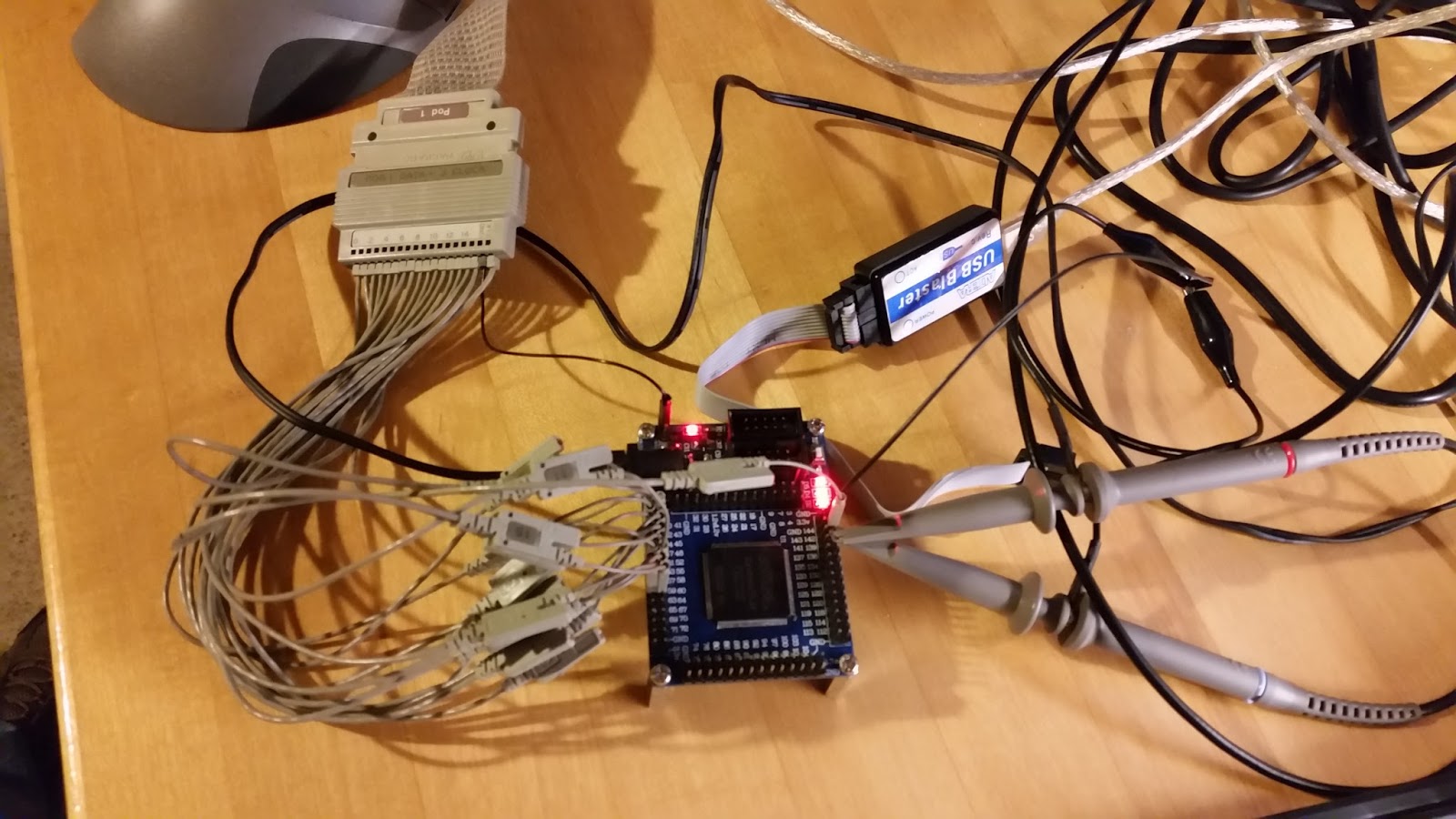
The board was setup to output the counter signals on pins 40-45, and the clock out on pin 143.  I didn't save this to the serial flash on the board, just ran it directly on the chip via the JTAG interface.
You can see the test setup below.

Test setup using FPGA board.

Pod 1 of the logic analyzer was hooked up to the counter signal pins as well as the clock out pin.
I also hooked up the channel one scope probe to the clout out pin, so I could view the analog clock signal.  Once the probes were all hooked up, I double checked that I could see signals on the analyzer. I setup the configuration, format, and triggers on the logic analyzer module to trigger on the counter signals from the FPGA.  After that I adjusted the settings on the oscilloscope module to make sure the analog clock signal was clearly displayed.  I then configured the scope to trigger after the logic analyzer in a group run chain.  You can see this in the screen shot below.

Intermodule configuration screen.

I ran a single shot group run to see what the time correlation bars would show, looks like they will capture almost the exact same instant.  Double checking the Scope module display proved that the group run triggering worked, you can see this in the screenshot below.

Oscilloscope capture from group run.
After a bit of playing around with the logic analyzer's user interface, I figured out how to add mixed signal information to the waveform display screen.  The below screenshot shows the counter signal output overlaid to display the count, the digital interpretation of the clock signal as well as the analog clock signal.  

Mixed Signal waveform screen.

This is a truly powerful setup, you can track digital logic glitches caused by analog signals this way.  Now, I wonder how difficult it is to work with the inverse assembler package....


Get the gunk out!

Since I acquired the HP 16500 C mainframe analyzer it needed some clean up.  I decided last night that I would clean it up a bit, since I couldn't sleep anyway.  The fans, and most of the case were covered in this greasy / sticky / nasty black soot like gunk.  I cleaned that off of every surface that I could, dried stuff off and re-assembled the analyzer.  Below are a few pictures I took during the process.

Main view of the chassis.

Power supply, hard drive and a fan bracket.

Side of CRT module and Fans.

Option Cards waiting re-installation.

Saturday, May 7, 2016

New useful additions!

In my previous post I mentioned the mainframe instrument I purchased.  I had another run of luck on eBay and was able to purchase a few more pieces.  I was able to obtain at 2 channel scope and a 102 channel logic analyzer card.

The oscilloscope card has good specifications: 2 channels, each with a 2 GS/sec 8 bit analog to digital converter. Each channel is capable of 500 MHz Bandwidth.  The logic analyzer card is capable of 500 MHz timing and 100 MHz state analysis with 102 channels.  The new configuration is shown in the picture below.

Current Configuration
The initial oscilloscope card tests were done using my function generator hooked up to both channels with the same signal function output.  In the screenshot below, you can see the 3 MHz sin waves shown on both channels.

Function Generator Scope Trace


I decided it to test out the new cards using an FPGA development board I have laying around.  I set up the design logic to output 16 signals for logic analysis as well as clock outputs for the scope channels.  A picture of the board setup to test the instrument cards is below.

Test Setup

I hooked up one of the flying lead pods up to the logic analyzer cable, then to the pins on the FPGA development board.  The oscilloscope probes and logic analyzer clock input line are connected to clock output pins as well.   I wrote some simple VHDL to synthesize some signals to test the logic analyzer and to output the clock signals.  The screenshot from the oscilloscope below shows that the clock output is 50 MHz.

FPGA Scope Trace

The clock signal isn't super clean and you would want to use a Schmitt trigger to clean that up before using it to drive something.  At least we can verify that the 50 MHz clock going into the FPGA can be forwarded out of the FPGA.  

The logic trace is very busy as you can see below.  The labels on the left side designate which pin on the FPGA development board the leads are connected to.

FPGA Logic Trace

The next thing for me to tackle is to figure out how to setup an inter-module trigger and run that as a group.  I know this will be useful in the future with some up coming projects.  Have fun everyone, see you next time.