This weekend I decided to upgrade the firmware in my home made power supply. I wanted to increase the stability of the voltage measurement and the response of the display.
Oversampling the ADC is how I decided to increase the accuracy and stability of the voltage measurement. I chose to use a new architecture, that utilizes a real time operating system. The first RTOS that came to mind for an 8-bit microchip processor was OSA RTOS. This is a wonderful, tiny RTOS that is meant to be used on very small processors, such as the PIC18F46K22 that is inserted into the READY for PIC board used in my power supply. I bought the board from MikroElectronika, just for this project. The below picture shows the power supply with the top open, you can see the READY for PIC board on the right near the back.
The firmware architecture is fairly simple, I used 3 tasks in conjunction with message passing.
The firmware entry point ( main ) sets up this architecture and then schedules all tasks, this can be seen below in the diagram.
The firmware first initializes the system, which consists of board support type operations such as LCD, ADC and Timer initialization routines. After this, the real time operating system is initialized, and the tasks are created. Once those steps are complete, we need to have the operating system enable all the interrupts, so that the scheduler can cycle between tasks. Finally, we enter into an infinite loop that will schedule time for each task in turn.
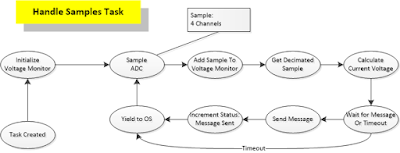
The first task, is also the most complicated one. The handle samples task, manages the ADC sampling, voltage monitor oversampling and decimation. This task actually samples 4 different ADC channels which all point to the same signal, this decreases the number of iterations
required to calculate the voltage value to display. The task makes use of a module called voltage monitor to handle the rolling over sample and decimation process. Once it has the decimated value, it checks to see if the message is available, and then sends the decimated sample if possible. In the event that there is a timeout while waiting for the message, the task will yield to the operating system scheduler. This can all be seen in the below diagram.
The second task, is the update LCD task. The diagram for this task is found below.
As you can see from the diagram, this task simply waits until there is a message to update the LCD.
If there is a message available; it will be retrieved, the voltage will be calculated, then output buffers will be built and displayed. Again, like the handle samples task, if the message is not available, the task will yield to the operating system scheduler.
The final task, the idle task is very simple. This is a task I used mostly for debugging the system. However in the future, it could be used to gather real time data about the system if I add more features. For instance, I could add PC based control of the power supply via a UART. There would be a task added to handle the commands from the UART, I could add a command to retrieve the diagnostic data from the global status structure. Currently, the idle task tracks operating system errors, operating system event errors, operating system messages received and sent. The flow of the idle task can be seen in the diagram below.
You may have noticed common theme in the way the tasks behave, namely that they always yield to the operating system scheduler as soon as they can. This promotes a fast responsive application. The task flow knows the best possible way to give control back to the operating system, so it is best to do that when possible.
As I worked on this project, I used a logic analyzer to capture start up to full task scheduling in the application. You can see that screenshot below, if you want to see a video of me talking about the power supply and this upgrade please use this link to view the video.


